Sunday 20 December 2015

Looking At A Cheap L-C Meter Kit From Ebay

In this video i take a look at a cheap (less than £10) L-C meter kit from ebay.

The 'M8' L-C Meter is an inexpensive kit from ebay, it has the following specifications:

Inductance Measurement Range: 0.1μH-2H
Capacitance Measurement Range: 1pF-2.5μF
Electrolytic Capacitor Measurement Range: 0.1μF-30000μF
Assembled Size: 8 * 8 * 1cm / 3.1 * 3.1 * 0.4in
Package Size: 14.5 * 11 * 1.5cm / 5.7 * 4.3 * 0.6in
Package Weight: 85g / 3oz


Wednesday 9 December 2015

Reforming Old Electrolytic Capacitors

Recently i had the opportunity to look at reforming of electrolytic capacitors that had been stored unused in a power supply.

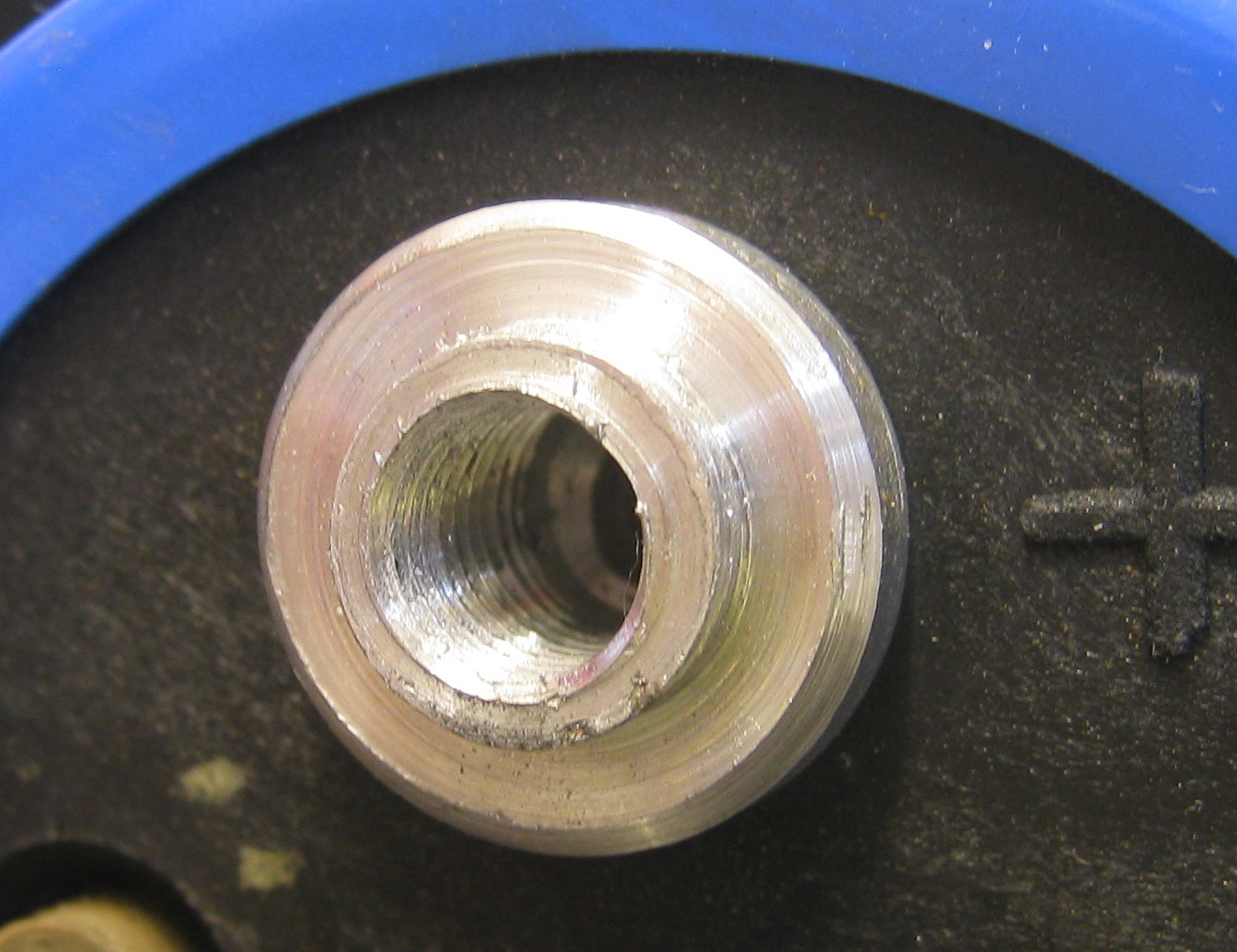
The capacitors in question are Cornell Dubilier Computamite branded FAH 42500-30-D3 which are 42,500uF 30V smoothing capacitors from a power supply that was dated March 1973, 42 years old at the time of this blog entry!


Computamite FAH-4425030

The capacitors were stored in-circuit with a bleed resistor of 10 kOhm, storage time was unknown but looking at the rest of the equipment i doubt they would have been used for at least 15 years, probably much longer.

Electrolytic capacitors work by storing a charge on two thin aluminium foil sheets separated by a dielectric material, usually paper impregnated with an electrolyte which is then rolled up into a cylinder and mounted inside an aluminium can with terminals for connection.

During the initial construction of a capacitor one sheet of the aluminium foil is processed to create an oxide layer on it's surface, this sheet becomes the Anode. The oxide layer is an electrical insulation layer between the anode and cathode and is the dielectric, this prevents electron flow and allows the storage of charge. This process is known as forming, the initial voltage is the 'Forming Voltage'. The thickness of the oxide layer depends on the forming voltage, typically the oxide layer is 0.0014uM per Volt so is extremely thin, even on high voltage electrolytic capacitors like large 450v bulk smoothing capacitors the thickness of the oxide layer would only be around 0.0005mm. The greater the thickness of the oxide layer partly determines the maximum voltage that can be applied to the capacitor without breakdown of the dielectric.


Electrolytic Capacitor Layers Showing Cathode And Anode

If capacitors are left for long periods of time, either in your storage bins, warehouses or even in manufactured products the electrolyte slowly erodes the oxide layer reducing it's insulating properties. If this is allowed to happen only for a couple of years then no issues will arise as the oxide layer will recover when the capacitor is next used. However over longer periods, especially on higher capacity and higher voltage rated capacitors they should be reformed in a controlled manner. Failure to do so may result in localised hot spots between the anode and cathode where vaporisation of the electrolyte can occur which leads to further damage of the aluminium foil.

With this in mind and reading about reforming capacitors in articles it seemed logical to limit the current flow into these capacitors and allow them to slowly build charge to the final voltage and allow the oxide layer to reform in a controlled manner.

Using my Keysight 6632B System Power Supply i initially charged the capacitor to 5V with a current limit of 50 mA. The advantage with these 42,500uF capacitors is their size, it means i can better see the processes involved as the time constant for charging means we have more time to see the process in action.

Initially i noticed that the capacitor certainly drew all the 50mA current available making the power supply operate in constant current mode, the voltage began to climb very slowly to 5V. This indicates the energy from my power supply was flowing into the capacitor but was not being stored as you would expect. I propose this energy was being used to re-establish the oxide layer.

Once the voltage reached 5V the current flow slowly reduced but did not fall to close to zero as i would expect. This indicates that either the capacitor is 'leaky' or as i suspect the energy was being used to reform the oxide layer. The still intact 10 kOhm bleed resistor would account for only 500 uA at 5V.

I disconnected it from the power supply and left it to discharge through the bleed resistor to about 500 mV and charged it again. This time the voltage rose much quicker than previously seen and after it was left connected for several minutes the final current draw was lower too and continuing to drop.

I repeated the procedure again; discharging and charging it but this time i set my power supply to 10V. During charging i noticed that the charge rose normally to 5v but then while charging to from 5V to 10V the voltage rose very very slowly again. I am speculating here that the oxide layer formed initially was enough to block a 5v charge but was not enough to block 10V and so over time the oxide layer increased to slowly block the 10v charge.

I repeated this process in increasing 5V steps, allowing it to take current at the set voltage for about 5 mins at a time until i was able to charge the capacitor to 30.5v and left it connected 'on charge' for several hours.

After finding a somewhat incomplete datasheet for this particular capacitor i went to test the ESR. This i measured using the same method as Alan Wolke (aka W2AEW) detailed in his video #135. After measuring the capacitor for after the treatment i found it's uF and it's ESR was right within specification.

Although these capacitors in question appear to have reformed very well i do not think i would really like to use these long-term given they are over 40 years old but it certainly proves the theory and practice for reforming very old capacitors.

It is vital to limit the current flow into the capacitor during the reforming process. If my understanding is correct this is more critical right at the beginning of the process. So i would recommend limiting the current to no more than 50mA (much less for smaller capacitors) and the voltage to 25% of it's rated voltage and allow it to charge and hold it at that voltage for 10 mins. Then repeat this process in 25% voltage steps until you reach it's operating voltage and then hold it there for 30 minutes.

During the holding time the current flow should drop to almost nothing. After the procedure measure the ESR, leakage and overall capacitance and compare to it's rated specification, if in doubt, discard the capacitor and use a new one.

Saturday 5 December 2015

Teardown: Grass Instruments Polygraph Mechanical Timer

In this video i take a quick look at a mechanical timer from the Grass Instruments Polygraph chart recorder.

We believe this opto-mechanical device is used to provide a two level pulse to put markings on the chart paper as it records.

The wheel is driven by a synchronous motor, it rotates at 12 RPM meaning the notches pass over the optical sensor every second with the bigger notch every complete rotation of 5 seconds.

The larger notch allows more light into the sensor so provides a bigger output and a bigger mark on the paper.

Wednesday 2 December 2015

Teardown: TEAC RD-111T 8 Channel DAT Data Recorder

In this video i play around and teardown a data logging device from the 1990s. A TEAC RD-111T DAT Data Recorder.

DAT or Digital Audio Tape was introduced in 1987 by Sony, originally designed for audio in this application it's being used to record 8 discrete channels of analog data.


Friday 27 November 2015

Teardown: Grass Instruments DC Driver Amp & Polygraph Integrator

In this video i begin looking inside some of the modules making up the Grass Instruments Polygraph.

Teardown: Grass Instruments Polygraph / EEG

This will be the beginning of a number of articles featuring the latest bit of hardware for teardown.

Although i had not intended to buy this particular item i managed to get a good price from the seller. Having previously seen it when i picked up another teardown item i knew it was loaded with lots of control knobs that would be worth money to the right people, not to mention all the metal so i took a gamble on buying it thinking it may pay for its own teardown.

I had to pickup in my van which was only just big enough and probably totalled around 300kg.

So the items i have consist of two polygraph machines the Grass Instruments Model 7D and the Grass Instruments Model 78 with chart recorders (oscillographs). There is also an additional chart recorder.

A polygraph is an interesting term, partly for the fact that it is commonly associated with lie detection, a procedure mostly used in the USA. A polygraph machine is not necessarily a lie detector. Lie detection is a technique that just uses a polygraph to monitor certain reactions to various questions, the operator is the one who decides if the person is telling the truth.

For the most part polygraphs are used in EEG (electroencephalography) which is monitoring electrical activity in the brain and also for sleep disorders amongst other medical uses. The polygraph simply takes very low amplitude signals from sensors attached to the skin, pulse rate, brain activity or other sensors that could monitor breathing or muscle responses. The signals are passed through amplification and filtering modules which then drive mechanical pens on a chart recorder. Modern machines would simply digitise the signals in a small box to be displayed on a laptop to dispense with the large machines featured here.

These polygraph machines were manufactured around the early 1970s, i say 'around' as many of the modules have slightly different dates of manufacture but seem to date between 1973 and 1981. They are from the Grass Instrument Co founded by Albert Grass in 1935.

Friday 20 November 2015

Minitron [Numitron] 3015F Vintage Incandescent 7 Segment Display

I recently found these Minitron 3051F displays in some equipment i dismantled.

The Minitron is a 7 segment display with a decimal point that uses small incandescent filaments made from Tungsten to form the segments. They are an evolution of the Numitron which works on the same principal but are packaged in the old 'valve' style glass packages. The minitron is packaged in a more modern 16pin DIP form like LED based 7 segment displays but with a borosilicate glass cover. Note the decimal point is an 8th filament but is partially masked off.

Operating these is very simple, the recommended operating voltage is 5v with each filament drawing around 8mA at 5v so can easily be driven directly from microcontrollers (making sure your accounting for the cold resistance and resulting current spike when they first turn on). I measured the current draw at 5v with all the segments on (including the decimal point) and it totalled 67mA. They have a surprisingly long life of around 50,000 hours at 5v.


Thursday 29 October 2015

Teardown: LeCroy HVL100 Discriminator Hybrid IC

I found this hybrid IC in the analog front end of the Packard Liquid Scintillation Analyser i took apart some time ago.

As it was a hybrid i saved it to take a look at in the future and today i removed it's cover to see inside.

The IC has a standard 16 pin DIL pinout but is an oversized package. The package is ceramic with bonded gold plated pins. The top cover is also ceramic which is glued on top of the main body.

The HVL100 is manufactured by LeCroy, famous for their high-end oscilloscopes and other test equipment. It is a discriminator and is a combination of the LeCroy MVL407 4 Channel Comparator and the Motorola MC10198 Monostable Multivibrator. The HVL100 here dates from 1996 and the following text is from it's datasheet:


Click Image To Zoom

After some heating with a hot-air gun i was able to remove the top cover.

Inside is a ceramic substrate with the components bonded to it and usual gold bondwires connecting the silicon devices to the ceramic substrate.

There are a couple of ceramic capacitors and two main integrated circuits, i would hazard a guess the central one is the main LeCroy MVL407 comparator , you can easily see the 4 sections in the die. The smaller device to the right is the Motorola MC10198.

Notice also the blue covering on some of the signal traces, generally this seems to be when a bond wire passes over the trace so maybe this is to reduce capacitance between the two traces?

Click Image To Zoom


Click Image To Zoom


Click Image To Zoom
Motorola MC10198. Note the copyright indication in the top right corner.

Click Image To Zoom
LeCroy MVL407.

Tuesday 20 October 2015

Tuesday 13 October 2015

Teardown: Vintage Solartron LM1619 Volt Meter

In this teardown i take a look at a vintage Solartron LM1619 Digital Volt Meter. This is a UK made product which dates from around the early 1970s.

Full Teardown Video:

The LM1619 is a 1999 count volt meter only with DC ranges of 200mV, 2V, 20V, 200V and 1kV. AC ranges are 2V, 20V, 200V and 750V.

The unit weighs about 5Kg and is housed in an extruded aluminium chassis with vinyl covered steel covers. The front panel is a thin layer of beige Formica with cutouts attached to the chassis. Has integral tilting bale.

Connections are provided on the front with three banana jacks, HI, LO & CHASSIS.

The display consists of three Mullard ZM1080 Nixie Tubes. Decimal places, polarity indication and the 1000 count indication are provided by discrete neon lamps.

Inside there are three main areas:

DVM Board
which contains most of the electronics for the voltage measurement. This includes two vacuum tubes, a Mullard CV4003 valve and a Mullard 83A1 which is the voltage reference.

Display Board
This contains the components to drive the three nixie tubes and consists mainly of descrete transistors on a hinged PCB for easy maintenance.

Front End
Located within a shielded can this houses the voltage dividers and trimmers along with a Weston cell and what appears to be a battery connection. Although the battery was missing from my unit i am insure what the battery was for.

View from the top:

View from the bottom.


Sunday 11 October 2015

Teardown: Avery Berkel D104 Post Office Scales

This is a short teardown of an Avery Berkel D104 Post Office Scales, as used in post offices throughout the UK.


The case is constructed of cast aluminium with a large aluminium bed, large 2x20 high contrast LCD display. The unit is intended to be bolted to a work surface.

Three data connections are located on the base.

Inside the unit the is the load cell, small mains transformer, and three significant PCBs, one has a selection of voltage regulators and analog circuitry for the load cell, the other two are what appears to be the digital processing board and then the display board.

Inside the unit, with the LCD & Display board removed from the front. The dataports are located on the far right. The digital controller board at the front, load cell in the centre and finally the analog board at the back. As shown in the picture below.


Below is the reverse of the display controller, the LCD module is mounted on the other side, with a IDC cable connecting on the right. It contains 64kbytes EPROM, Intel 8032AH Microcontroller, SRAM, Intel n825306 Serial Communications Controller and two MAX232 RS232 drivers. There is a small power supply section at the top left as this board runs from a separate transformer tap so is isolated from the other boards.


Below is the analog board, power supply regulation on the left with discrete diode bridge rectifier and linear regulators for the voltages needed for the analog side. The analog front end for the load cell is located in the area to the right where i have removed the shielding can.


The digital board below takes a IDC cable from the analog board, located at that connector is a custom ASIC and an 32kbyte EPROM. Also on this board is another Intel 8032AH microcontroller, MAX232 RS232 driver and four opto isolators. I would guess these are for the three external ports and the internal display board which uses RS232 between the two boards.


The load cell below is a 6kg rated device, no manufacturers name can be found on it, given Avery Berkel's size this could be of their own design.


Saturday 19 September 2015

Magstim 200 Hacked: Charging & Triggering Success!

So it's taken a couple of months to figure this Magstim 200 out and i have finally made it charge, trigger and discharge the capacitor.

After my last blog entry where i had disabled the 'Replace Coil' error / interlock by brute-forcing the PAL (Programmable Array Logic IC that seems to control the final safety interlocks to find the correct combinations that would disable the lock, this worked but left me with the device unable to trigger.


The PAL IC on the breadboard along with a binary counter IC (Motorola MC14060B) 
to run through all the 512 combinations of logic inputs to find the state that would disable the 'Replace Coil' error.

You can see on the scope picture above the top trace is the 4th stage counter output to the PAL, the other stages connect to each of the other PAL input pins so it will cycle through every combination as the counter (a Motorola MC14060B) counts upwards. The 2nd lower trace is the output pin that controls the replace coil error, so this is showing there are only two input states that bring the coil error output low indicating a fault.

Note there is a total of 512 output states from this PAL IC but not all the input pins will be applicable to this output condition. Clearly you can see there is only a few input states that control the output which is why there is only 9 clock cycles before the pattern repeats.

I simply clocked the counter first at high speed (a 100khz or so) watching the output on my oscilloscope in roll mode to first check the coil error state does change, then slow down the clock (to just a few hz) so i can stop it when it's in the output condition i want. I can then read off the state of the inputs. This can then be compared to the states seen when the IC is in the actual magstim board when the error is showing. In my case pin 5 was low and should be high. Disconnecting the input pin from it's source and bringing it high removes this lock.


Bodge wire from VCC to pin 5, this should be pulled high to disable the interlock. The bodged on resistor is from the factory!

I also look at the charge voltage of the capacitor, i see a maximum reading of around 1700v, this is less than i expected. In the documentation i have seen from Magstim it indicated it would be around 2800v as seen in this excerpt from "Guide to Magnetic Stimulation" by Reza Jalinous:-


Full video after removing the interlock:


I spent much time tracing the trigger circuit, and found the front panel board supplies 5v to the trigger input of the potted trigger block. This is pulled low by the front panel trigger button only when pin 'K' on the front panel connector is also pulled low to ground.

This pin would be for the interlock switch located on the Magstim coil itself, intended to be held in by the operator when they are ready to trigger the device. So typically they would place the coil where they wanted, hold in the coil interlock and then either press the front panel 'Trigger' or depress a pneumatic foot switch to actually trigger the unit.

So a simple fix, once this was discovered i could remove the multi-way connector from the front panel and solder a bridge wire across those pins on the front panel board.


Bodge wire to remove the coil switch interlock.

In the future i will make some binding posts for the front panel to allow easy connection and disconnection of things i want to blow up or experiment with.

So currently the unit will charge the capacitor to about 1700v in 1% steps. I have done some measurements of this and found the accuracy of this is very approximate and certainly at the higher charges the charge leaks away requiring the unit to keep topping up the capacitor. At the higher voltages the hysteresis of this can be as much as 40v or so. At the moment i am not sure if this self discharge is natural leakage in the capacitor or other parts of the circuit.

At 100% the capacitor is charged to about 1680v so has about 268 Joules of energy stored. The lowest power (1%) will charge the capacitor to about 40v which is 0.15 Joules. The scaling of the % power value to the actual voltage is non-linear, certainly at power levels below 30%. Upto 30% it is much better, at 30% the charge will be about 525v which is actually closer to 10% of full power. Above the 30% the power does rise in more linear fashion to 100%.

The capacitor seems to measure 190uF and is oil filled. Magstim rated the capacitor to a minimum 200,000 full charge cycles. Quite impressive for what it does. I would expect the capacitor was a significant part of the BOM for this device along with the Thyristor. The capacitor i believe is a General Atomics DP Series 39504 which are general purpose pulse capacitors capable of upto 25kA. The 39504 is rated at 185uF at 3000v.

I have also noticed that the mechanical counter only counts when its triggered at over 80% power.

Power Levels vs Voltages vs Joules
1% = 40v = 0.152 Joules
25% = 425v = 17.1 Joules
50% = 850v = 68.6 Joules
75% = 1,275v = 154.4 Joules
100%  = 1,680v = 268.1 Joules

Full video after i resolved the triggering issue:

Friday 28 August 2015

Magstim 200: HV Charging & Control Boards

Following the teardown of the Magstim 200 TMS device i featured on my youtube channel a few weeks ago i have been slowly de-potting the two (what i call) bricks.

The two devices seemed to control the charging and discharging of the main HV capacitor in the device. Although i could infer their purpose i did want to explore further.

The first brick to get some treatment was what appeared to be the charging brick, firstly i used a hot air gun, this seemed to work well initially by softening the potting compound but the effect only went a few mm deep but it did reveal some components.

Thanks to a couple of comments about how to better remove the potting compound i ordered a litre of Dichloromethane, removed as much of the external packaging as much as i could and immersed them.

After a just hours the first brick softened and i was able to remove enough of the compound to discover it's operation.

The connections across the top are 240v AC IN from the supply mains, which is switched through two Solid State Relays operated by the main control board. The output is fed to the primary of the HV transformer.

The secondary of the HV transformer runs through a set of external power resistors and back into the HV AC IN of the charging brick where there is a bridge rectifier consisting of 8 discrete diodes. The output of the rectifier runs through 4 power resistors to supply rectified HV to the remaining connector on the power brick (HV DC OUT).


The other brick which i see as the charging & triggering brick is more complex with 6 connections, it was potted with a different material and took much longer to come off, i wasn't able to remove all of it as i ran out of dichloromethane but it was enough to see what each of the connections did. The High Voltage DC from the charging brick connects to two connections and also pass through to the main HV capacitor. The positive is internally connected through two 30MOhm resistors to what i suspect will be voltage monitoring feeding back to the main control board. The negative side of the High Voltage DC seems to connect internally to the SCR switching outputs. The final connection is clearly a low voltage input control from the main control board. It took over three weeks in Dichloromethane to reveal this.

Saturday 25 July 2015

Teardown: Magstim 200 TMS Transcranial Magnetic Stimulator Base Unit

In this video i disassemble a Magstim 200, this is a TMS device manufactured in the late 1980s. Production began in the mid 1980s and ran through until at least 1999.

TMS is a medical technique to stimulate the brain and nerves throughout the body using a closely coupled induction coil placed on the head that is energized with a short duration high voltage/high current pulse. The magnetic field from the coil induces small currents into the brain or nerves through the skull and skin.

The Magstim Company was founded from research performed at Sheffield University during the early and middle 1980s.

I recently purchased two used Magstim 200 base units for teardown. One appears to be working and dates from the late 1990s, the other is broken and dates from the late 1980s. It's the broken one i teardown in this video.


Saturday 11 July 2015

Repairing An M5 Thread On A Capacitor

I salvaged four capacitors from the Red Light Camera i did a teardown on a while ago. I found when i removed them that one capacitor had one thread completely gone. It looks like it might have just been over tightened at the factory.

The damaged thread.

I opted to try and Helicoil it, i have used them before to repair larger threads like M12, the capacitor uses two M5 which are much smaller but i thought i would give it a try.

The procedure involves buying a kit which contains the coils, drill, tap and a couple of insertion tools.

The first step is to drill out the old thread with the included drill bit then you tap and then insert the coil. The coil becomes the new thread at the original size.

In this instance there is a small issue in that these are not really designed to be inserted into shallow blind holes, you need enough depth to get the drill in and the tap has to work to a minimum depth to cut the thread.

So first off i ground the tip off the drill and the tap so i can work with a shallow hole.

Drill and Tap with ground ends.


After drilling out the old thread.


Cutting the new thread with the supplied tap.


The new intermediate thread for the coil.


The coil on the insertion tool. The coil will become the new M5 thread.


Inserting the coil. It simply screws in.


The end result, a new M5 thread that will actually be stronger than it was originally.

Saturday 4 July 2015

Midland G9 PMR446 5 Watt Full Power Export Modification

In this article i will detail how to convert a normal Midland G9 Plus or G9E Plus 2-way radio to the export version that has enhanced 5 watt output. It also allows the two PTT buttons to be used to operate the radio in standard 500mW and in 5000mW.


The modification is quite simple on this 2015 version Midland G9E Plus.


Take your Midland G9 and remove the belt clip and batteries. You will find four screws located in the battery area and one next to the belt clip. Carefully remove these with Philips screwdriver.


Open the cover carefully, note the wires to the vibration motor, these can easily be broken if they are pulled hard.


At the top of the PCB next to the On/Off/Volume control you will find three jumper links labelled J-1, J-2 & J-3.

To make the modification, simply cut links J-2 & J-3. 

The radio can be re-assembled. When you next turn on the power the settings will reset to factory default.

The radio will operate as it did before but with the exception that the PTT & PTT Boost will work differently. In the menu if you change PRL setting to be 'L'. This will make the PTT button transmit at 500mW and the PTT Boost button will transmit at 5000mW.

Other Notes:

The radio seems to be operated by a Beken BK4811 transceiver IC.

Power consumption measurements at 5.00v
Idle: 78mA
Idle + Backlight: 95mA
TX 100mW: 170mA
TX 500mW: 470mA
TX 5000mW: 980mA

I also made some measurements of the battery level indicator:
Full battery indication at 4.77v+
2 bar battery indication at 4.72v
1 bar battery indication at 4.5v
Bat Lo warning at 4.3v


Sunday 28 June 2015

Archiving Hi8 Video Tapes to MP4

So recently i was reading up about the Hi8 Video tape format, this is what i used to use back in the 1990s and 2000s with my Sony TRV-66E camcorder.

I have a significant amount of old tapes that never get played and read that the Hi8 tape format is prone to degradation after about 15 years.

So with that in mind i began to transfer my tapes into H.264 / AAC streams for proper archiving and uploading to YouTube, so these are my experiences.

Tape Degradation
I have viewed some of my tapes and some do show some form of playback artefacts. As you can see in this picture below the bottom half is affected by distortion and horizontal sparkle effects and runs throughout the entire tape. Visually there is nothing visible on the physical tape itself.


Digitizing The Media
This is a lossy step in the process, that means you can affect the quality of the final recording depending on how you do this.

I dont have a PC based video capture device, it's not something i have needed before. I have used them in the past (during the late 1990s and early 2000s) with mixed results, maybe better products are out there now but i generally dont like them!

I do however, have a decent quality hard disk based DVR and DVD writer (a Sony RDR-HX710). This will allow me to record my tapes into an MPEG2 stream either directly onto a DVD+R or to the internal HDD for later transfer to DVD+R.

The DVR can accept analog video in the forms of composite or  S-Video. S-Video is obviously the preferred format here as it separates parts of the video signal to retain more detail.

Because the DVR has only a single layer DVD writer i am limited to standard 4.7Gb DVD+R or DVD+RW so i need to try and fit one whole Hi8 tape onto one DVD. I want to make the 90 minutes fill the disk. If you encode the tape so it only fills 1/3 of the DVD your effectively losing quality because you may find a slightly high recording quality in the DVR settings that could fill the disk with nothing left over.

After some testing i found the most efficient way to record the tapes was to write DVD+Rs directly. This saves me time as there is no HDD -> DVD recording process. I also found using the DVR quality setting on 'HSP' (this is only a Sony naming convention, yours may be different). This encodes at about 7.7 Mbps.


Using the DVR is great, it means i can set play/record and leave it to finish,  it doesn't tie up my PC for hours and i don't have to worry about wonky capture device drivers that will drop frames if you so much as look at the PC the wrong way, or audio that drifts out of sync. It also means i can just archive my tapes onto many DVDs that can be ripped and edited at a later date. In addition to this the output is pure PAL standard 720x576 25FPS Interlaced.

Transferring to PC
This part should have been the simplest, but in reality it was not but in a way it helped the process in a funny way.

After the DVD is written and finalised i can take the DVD and read off the files on my PC. All DVDs are readable this way with the exception of copyright protected disks that have their files encrypted. Because this is an original recording from my DVR there is no encryption so the files can be copied without any issue.

The files that contain the actual content are the VTS_01_[X].VOB located in the VIDEO_TS folder. Copy and rename these on the PC to .MPG and they will play in most media players.

This is where i hit my first problem, for some reason the first VOB file wont play in VLC or load into Movie Studio. It's corrupt or badly formed in some way. It plays fine on the DVR and in Windows Media Player. Thankfully it does load into Handbrake. I have transferred recordings using this method before without issue so i may look into this further to see which bit i'm doing is causing the problem.

I wanted to edit and make the final videos from this original MPEG2 source in Movie Studio but there was a lot of noise in the encoding, small MPEG blocking artefacts and high frequency noise from the original tape and i had this issue with the corrupt file. Movie Studio has little or no options for removing blocking artefacts or noise too so i needed another solution...

After some experimenting i found i could encode these MPEG2 streams into MPEG4 using Handbrake which can read the corrupt file and apply some additional processing to reduce some of the artefacts so in a way it helps even though it adds an additional encoding step and more time to the process. So my handbrake settings were as follows:

Picture Tab: 

Anamorphic: Strict
Cropping: custom, set to zero. Handbrake does a poor job of cropping and i prefer to use the pan/scan options in Movie Studio. So i disable this option, annoyingly it will always revert back on any new video.


Filters Tab:
Deinterlace: Fast, being an original PAL source the picture is interlaced so  this should be removed prior to encoding into the final video.
Deblock & Denoise: Off

Video Tab:
Quality: 12
Constant Framerate: On
Framerate: Same As Source
x264 Preset: Medium
x264 Tune: Grain
H.264 Profile: High

Alternative Method, less filtering, lower compression.
This method i disable the deblock and denoise functions and increase the compression Quality enough so the inherent grain is retained. This actually looks more natural. There is a balance though, you need enough quality to resolve the noise. Not enough and the noise will turn into very obvious blocking itself. In my tests a Quality setting of 12 and disabling the deblock and denoise functions.

Final Differences
I was going to include some half and half images between the MPEG2 and MP4 versions but the differences are so subtle i doubt you would be able to see them. It really is just some high frequency noise.

Editing
The original MPEG2 .VOB files are around 1Gb in size, after conversion to MP4 they do increase to more than 2.5Gb, i found this was inevitable to retain the grain, this is only an intermediate format for editing though. Once the videos have been rejoined, edited, cropped and some basic level and gamma correction they are exported from Sony Movie Studio as a 5mbps MP4.

Thursday 18 June 2015

Update: 1980s Digital Video Effects Processor

Just some small snippets of extra information about the CEL Electronics P164 & P152B video effects combo:

The P177 connector at the back is for the 'P177 Component Combiner'.

Also additional devices related to this are the 'P158 Eric Editing System Machine Interface' and 'P163 Digital Effects Controller'.

The P164 & P152 form a system called the 'CEL MS850B Effects System', other variants of this are the MS851B with the addition of a BIM (Built In Mixer) and the MS852B which is basically one P152 Touch Screen Controller and two P164 DVEs with the BIM option. The touch screen controller can operate multiple P164s at the same time.

After some lengthy reading about similar DVE systems from Quantel, Sony and Abekas during the mid-80s i believe this is run of the mill system. Maybe offering similar performance to these other high-end and seriously expensive systems but at lower cost. Given it's date (the user guide is written in 1990) it does seem somewhat lacking in capabilities. But this remains somewhat unknown until i can get the system running.

If anyone has any information about any of these devices, please let me know by leaving a message in the comments.

P152 & P164 EPROMs

I have also dumped all of the EPROMs from both the P152 and P164. Interestingly the P164 does have a number of ASCII text strings contained in the CPU Board EPROMs.

ROMCP0 & ROMCP1 are interleaved so the two 32kbyte EPROM dumps need to be merged to form a single 64kbyte binary.

The strings seem to relate to a DSP programming or debug interface as these code snippets show extracted from the CPU board EPROM.

H-help: M=modifyD=dumpF=fill PROGRAM
m=modifyd=dumpf=fill DATA
R=regdumpG=gotoK=code upload
B=set breakpointC=continue
I=int enableX=int disable
Z=disassemble
>>> TMS320C25 Diagnostic Kernel V9.0 <<<
NO 16k- 32k- RAM system
EPROM ID: Storage Processor DPRAM
** TEST OK **
EPROM boot block not found
AUTOBOOT DISABLED
Non-volatile RAM is corrupt
DISASSEMBLE
Serial Ports
I have connected to all of the serial ports available, all those on the P152B do nothing as i expected. The 'Controller' port on the P164 makes my USB->RS232 adaptor drop its USB connection so may not be RS232 but the 'Panel' port outputs a continuous stream of '[00]' at 9600/8/N/1